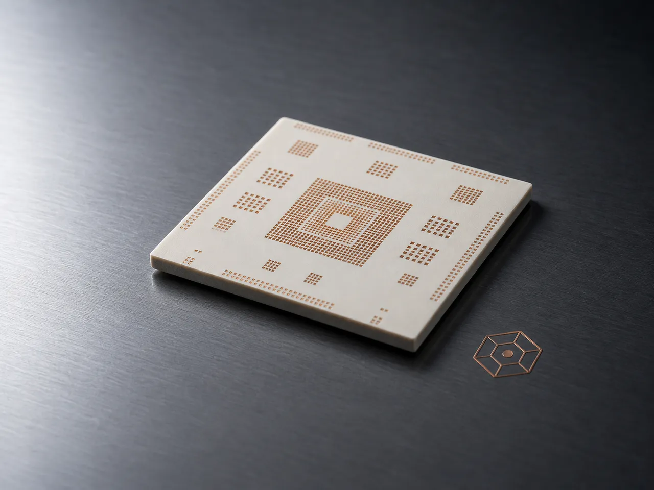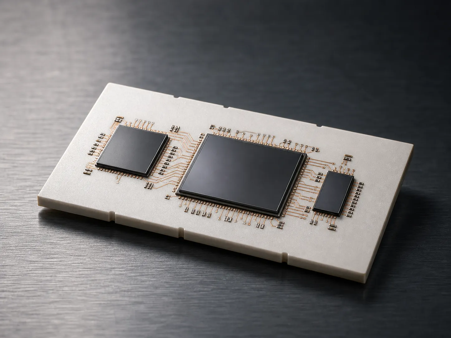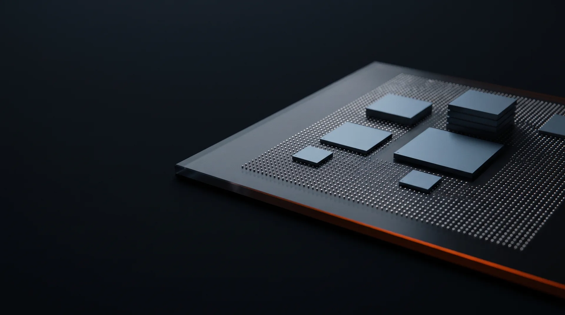
Adjustable ceramic substrates for the next generation of advanced packaging.
Active R&D, thermal conductivity characterization in progress. Discuss the current envelope with our materials team.
Two applications in validation, from chiplet carriers to co-packaged optics. Each one starts from a die stack, not from a grade.
Advanced packaging is a dimensional problem. A 2.5D or 3D stack bonds materials with different expansion rates: silicon sits near 2.6 ×10⁻⁶/K, organic laminate around six times higher. Every thermal excursion in assembly and in service works that mismatch.
What it costs is measurable. Warpage at reflow, die shift, stress concentrated at the interconnect, and yield loss that scales with package area. As packages grow toward panel format the mismatch stops being a tolerance question and becomes the limiting factor on how large a package can be built.
The industry response has been to move the substrate toward glass, for modulus and expansion rather than for heat spreading. That direction is correct and the reasoning is public. What has not changed is that published low-expansion materials still arrive as a fixed value, and a stack that mixes silicon, GaN and SiC does not have one expansion target.
Tunable CTE matched to the semiconductor stack, not the other way around.
Coefficient of thermal expansion formulated to your die stack rather than selected from a fixed grade, and adjustable across 100 to 800 °C so the substrate tracks the package through assembly and through operation. Composition α-Al₂O₃ + boron-based additive. Supplied as a ready-to-fire powder blend, so panel format and via strategy stay yours. Thermal conductivity and GHz-band dielectric characterization are in progress; current data ships with the qualification package.
Full Adaptive Glass-Ceramic specEngineers working on advanced packaging often also evaluate Strocera in AI Infrastructure for power module and RF substrates, and Strocera in Space for dimensionally stable optical structures.
Bring the operating conditions. We'll tell you which platform fits, and how we'd formulate it.
Talk to materials engineering